Smartwatch: ATMega328P design vs RP2040 build
2026-08-04
Throughout my studies and career so far, I have rebuilt a smartwatch twice. Initially I did this as my Extended Project Qualification (EPQ) during my A-Levels, and then I revisited the core idea during my Electronic and Electrical Engineering degree as my final dissertation but with a machine learning twist. I repeated the same core idea because it gave me a clear comparison to myself four years prior.
The second version showed clearer hardware improvements, and now I am designing a version 3 to showcase the software skills from working as a software engineer for a few years. I’ve always felt the UI and software in general could have been more refined.
Same product three times, each shows the progression in the intervening years: 2018 to 2022 measures the EEE degree, 2022 to 2026 measures the job.
Version 1, EPQ (2018)
EPQ Report (PDF) | EPQ Presentation (PDF)
For my A-level EPQ I designed a smartwatch from scratch in EasyEDA, which was an ATmega328P with a 1.3-inch OLED display, Bluetooth LE, and a proper LiPo charge path, benchmarked against the Apple Watch 3 and Pebble Time. Every part got picked the slow way, from datasheets: I compared three AVR micros on their supply current curves, chose Bluetooth over Wi-Fi because 17 mA beats 170 mA, and took the DS1338Z-33 RTC over the usual DS1307 because the DS1307 is a 5 V part and my rail was 3.3 V.
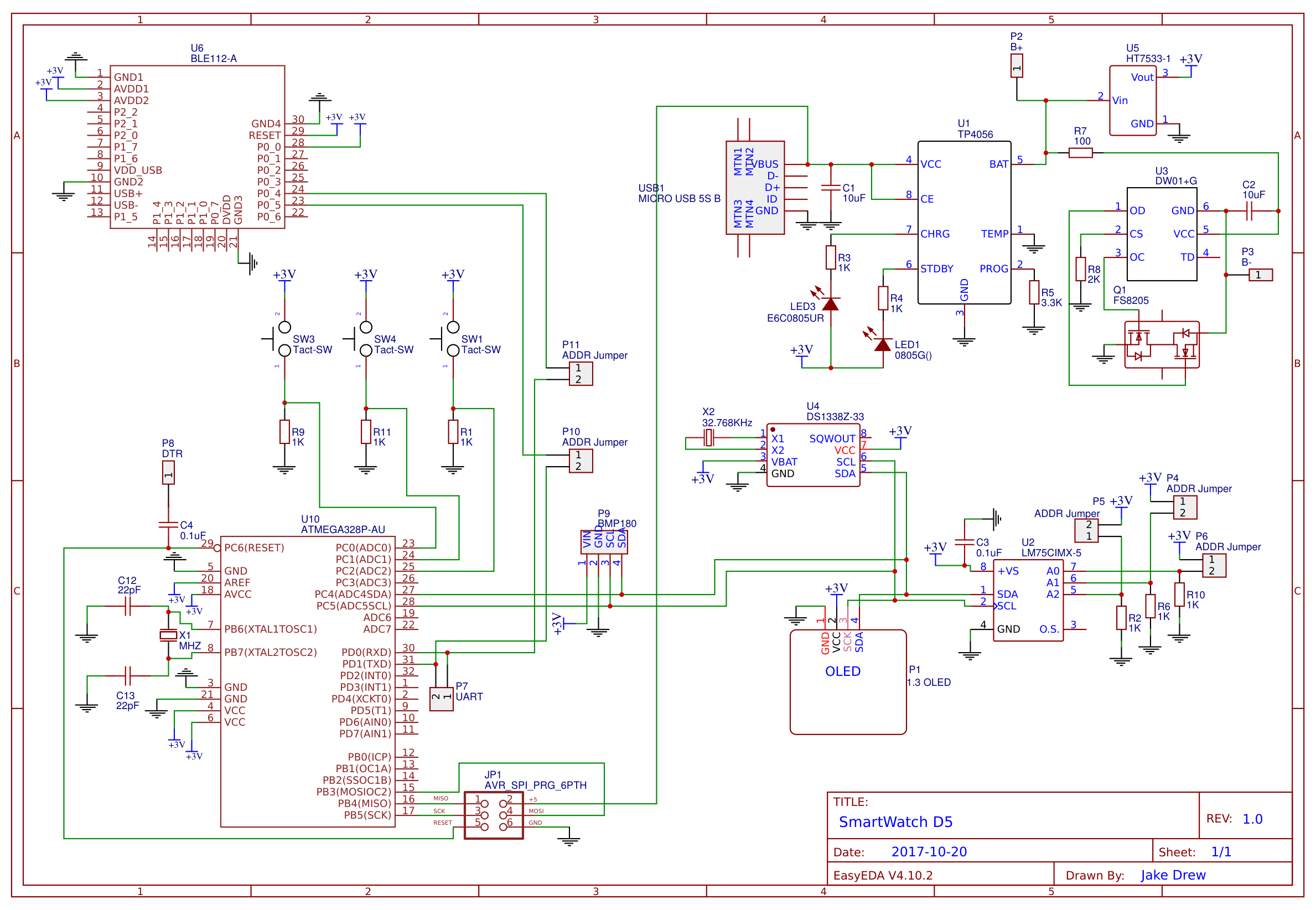
The design went through five revisions in three months, I started with an IMU, SPI flash and haptic driver which were all in revision D2 and all cut by revision D5 (Dx was my versioning scheme). This resulted in a £27 BOM against Apple’s £329. I exported Gerbers and had eight boards fabbed for £4.63, and they were delivered in five days:
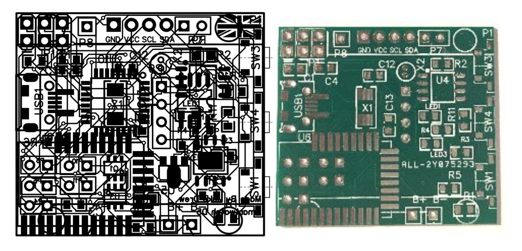
They were never populated: I had prototyped the peripherals on a breadboard testing the communications to my Arduino Uno (uses the same ATmega328P chip), so the watch board never ran at all, and every power figure was calculated rather than measured. This is reflected in the project name “To design a smartwatch and evaluate it against commercial alternatives.” it was a design, not a device.
Version 2, Dissertation (2022)
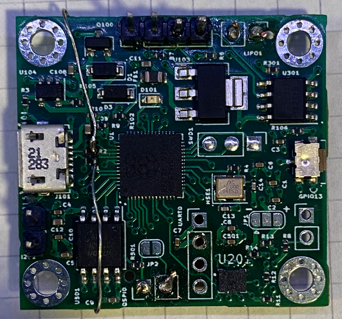
The dissertation rebuild was the same product done properly: an RP2040 (chosen at £0.52 against a £4.39 STM32), laid out in KiCad on four layers and assembled by JLCPCB, this time I went with everything machine placed on one side so JLC could assemble the majority of the board. This allowed me to use parts which would’ve been pretty hard to do reliably without the use of a reflow oven. I could also shrink the resistors to 0402s throughout. The chip shortage forced me to swap the IMU mid-project when Farnell’s MPU6050 lead time blew past my deadline, so an LSM6DS3 went in instead.
Firmware was embedded Rust on rp-hal, a year into that ecosystem existing, running a DeepConvLSTM classifier I’d validated at 83.2% on a 1.8M-row UCI dataset, and deployed with TensorFlow Lite Micro on the watch.
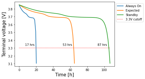
Battery life was simulated with PyBaMM from per-state current tables, 57 hours expected against a 2-day requirement:
The boards came back with 27.4kΩ for the USB termination but this needed 27.4Ω, my ordering mistake. This board revision was saved by the test pads I’d put on the underside “just in case” I needed to debug the USB which I could then connect some through-hole resistors to and then post fabrication fix this termination value. The one thing I still didn’t get done: no radio (WiFi/Bluetooth) made this board.
What’s next
v3 is in design now.
Changelog
2018-01-04 V1 Design complete, D5 schematic and Gerbers exported
2022-05-03 V2 Dissertation Submitted
2026-08-04 Note published